Silicon photonics has shown potential for low-cost large-scale photonic-electronic integration. Silicon micro/nano-structures offer novel mechanisms to improve the performance of conventional silicon photonic devices as demonstrated in our prior work (e.g. photonic crystal waveguide modulator). These efforts also brought us fundamental understanding of current density scaling and power consumption of silicon electro-optic devices, as well as heat transfer in silicon thermo-optic devices (e.g. using the “image charge” analogy). Considering the challenges of reliable manufacturing of active silicon photonic devices in real applications, we also initiated the study of fabrication variation of silicon Mach-Zehnder modulators recently.
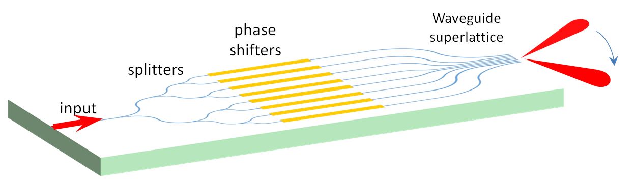
Furthermore, recent efforts on high-density waveguide integration open the door to high-performance optical phased arrays (OPAs) with potential applications in LIDARs for self-driving cars, high-density optical interconnect and space division multiplexing. When the low-cost large-scale monolithic integration capability of silicon photonics meets the intriguing physics in novel micro/nano-photonic structures, an area of abundant opportunities is unfolding. To explore these opportunities we need innovative ideas, practical rationale, physical insight, efficient simulation/modeling, and careful fabrication and characterization.
Photonic crystals and optical metamaterials research had exciting development in the last two decades. Built upon many advances in physics and materials, nanophotonic devices such as lasers and modulators have been demonstrated recently with orders of magnitude better performance than their conventional counterparts. Looking ahead, challenges remain in reducing slow light loss, further reducing device power consumption, exploring some fundamental limits. We contributed to some of these past efforts, such as photonic crystal waveguide (PCW) modulator, slot PCW, superprism, and slow light loss. Occasionally, these highly challenging problems stemming from device research also brought deeper understanding of some foundational problems in solid state physics, such as wave transmission through the surface of a periodic lattice with arbitrary Miller indices (including irrational Miller indices), and the cross-sectional eigenmode orthogonality in 1D-periodic structures in 3D space (e.g. PCW).
In these studies, we often combine theory and experiment, connect fundamental/device physics to engineering perspective to obtain a holistic view of the problem and seek a meaningful solution. You are welcome to browse through our work on this website, and uncover your own new paths in these areas.
(Scroll down, to see research topics below)
High-density waveguide integration & Optical phased array (OPA)
* High-density integration is the trend for silicon photonics. Integration density of waveguides—the most ubiquitous components of Si photonics, is crucial.
* Challenge: strong coupling as waveguides get close
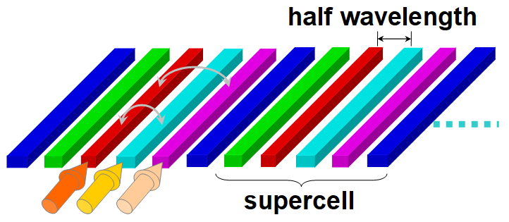
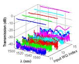
* Introduce a waveguide superlattice to suppress waveguide coupling at submicron pitches.
* Achieved high-density waveguide array at half-wavelength pitches, crosstak <-20dB. : Nature Comm. 2015, PhotonRes 2016, Optica 2019
* Applications: (1) Optical phased array for LIDAR; (2) Space-division multiplexing (SDM); (3) High wavelength resolution (or compact) spectrometer & WDM demux. .
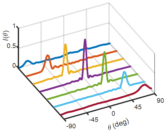
* Demonstrated half-wavelength pitch superlattice optical phased array with angular steering range 150deg, main beam engery ratio up to 83%, sidelobes < -12 dB over 180deg field, waveguide crosstalk < -20 dB: Phys. Rev. Appl. 2021
* Neural network based phase calibration for OPA: Photon. Res. 2022
* Independent multiple beams generated by OPA: LPR 2026, OE 2025, COL 2024
* Application: Mobile Wireless Optical Communications: OL 2024, LPR 2026
* News: Phys.org, NJU press release 2021, Adv. in Eng., NJU news 2024, COL Editor's Pick, NJU news 2026
* Patent: US Patent No. 9784914 (2017)
Optical Computing & AI
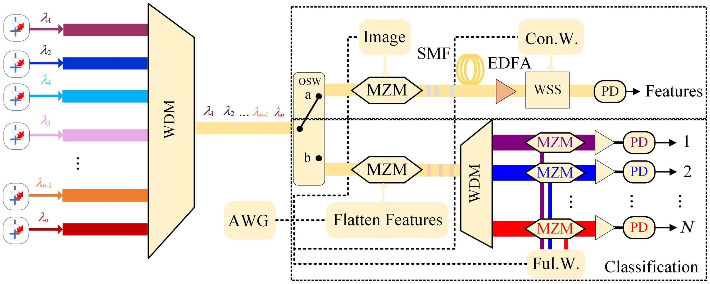
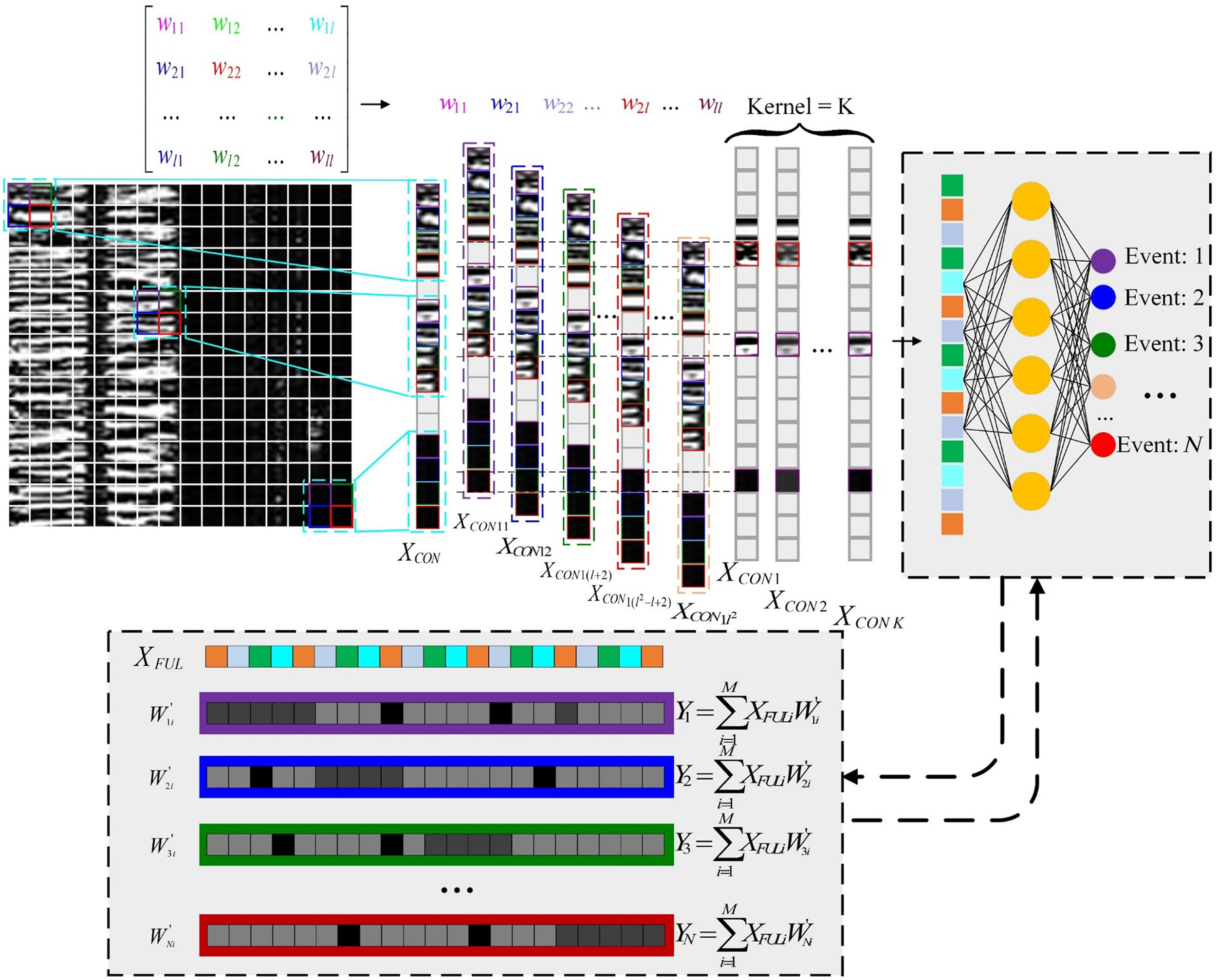
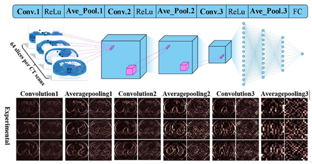
* Photonic neural network accelerator for convolution and full connection
* Photonic tensor processing unit with single dataflow & programmable high-precision weighting control
* Reduce RF/High-speed devices used in such photonic computing by several times, significantly reduce cost
* Potential application: fiber-optic sensing, diagonsis of disease (e.g. COVID-19) via CT scans
* Publications: AdvPhoton2025, JLT2024, OE2023
* News: NJU press release
* Use of artificial neural networks for phase calibration of optical phased arrays
* Publications: PhotonRes2022
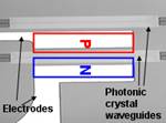
Silicon modulators based on photonic crystals
* The first GHz photonic crystal waveguide modulator
* Scaling law for the electric current density of high-speed silicon modulators (leading to prediction of power consumption)
* Publications: APL07, SSE07, JSTQE08, ..., JPhysD23(review)
* News reports:
Nature Photonics: Research Highlights,
NASA Tech Brief, Laser Focus World, more...
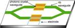
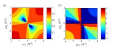
Dual racetrack micro-resonator modulator
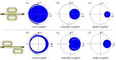
* Strong coherent cross-coupling between two parallel racetrack micro-resonators
* In over-coupling scenario, there is a delicate balance between the direct sum and “interactions” of two resonances
* Large amplitude & phase modulation ranges
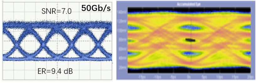
* Suitable for DAC-less PAM & coherent modulation (including DPSK, QPSK, 16-QAM, etc.)
* High extinction ratio 9.4 dB & high signal-to-noise ratio 7.0 @ 50Gb/s experiment with Vpp=2.3V
* Capable of low-chirp modulation, outputting 100Gb/s for 2km transmission
* Resilient against fabrication imperfections
* Publications: OE2011, OL2022, JPhysD2023, JLT2025
* US Patent No. 9,239,477 (2016).
* News: NJU News
Silicon thermo-optic devices
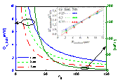
* Demonstrated high extinction ratios (avg. >35 dB over 60nm band) for all 4 paths of 2x2 thermo-optic switch with a parabolic MMI: PTL2023
* Analytic theory of silicon thermo-optic devices using "image charge" analogy: PTL2019
* Analytic theory of silicon thermo-optic devices based on photonic crystal waveguides: OE2012
* Power consumption and spatial temperature profile are found as explicit functions of structural, thermal and optical parameters
* Agree with FEM simulations and experiments
* Air-bridge (membrane) configuration is shown to enhance the temperature rise compared to the SOI structure.
* Scaling of power consumption with key parameters (buried oxide layer thickness, heater location & width, group index, etc.)
* Substrate effect of SOI thermo-optic devices can be precisely modeled: OE2013
* Related experimental publications: PTL2007, PJ2018
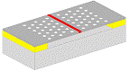
Photonic crystal interface physics (including superprism effect)
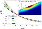
* A general theory of wave transmission through a surface of a periodic structure—for any surface orientation (either periodic or quasi-periodic surfaces, i.e. rational or irrational Miller indices): PRB2005
* Rigorous formulas for superprism sensitivities: PRB2008
* Synegistic theoretical framework of slow light and superprism effects: JNN2010
* Treatment for 1D cases (gratings) & 3D photonic crystals: JOSA-A2006, JLT2007
* Related experimental publications: JAP2007
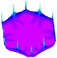
Symmetry in Multi-dimensional Photonic Crystals
* Symmetry plays important roles in designing photonic crystal structures and devices or, more generally, 2D/3D photonic synthetic structures.
* Even-Odd mode-symmetry/parity transform in PCWs shows the potential of breaking time-reversal symmetry, enabling one-way waveguides or optical isolators.
* Symmetry-induced singularities can lead to ultra-high sensitivities in superprism effects while maintaining low loss.
* Symmetrical structures can enable a class of novel wavelength-division-multiplexing (WDM) devices.
* Publications: OL12, OE13, PRB08, PRL03,
* US Patent No. 9,086,583 (2015).
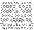
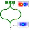
Slot photonic crystal waveguides
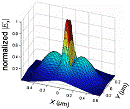
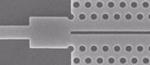
* Strong optical confinement (lower figure) and slow light enhancement
* MMI coupling scheme (upper figure)
* High-speed Si MOS modulator demonstrated
* US Patent No. 7,421,179 (2008).
Slow light loss in a photonic crystal waveguide
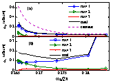
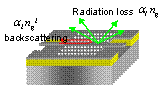
* Analytic theory reveals general characteristics of slow light loss
* Loss dominated by random scattering of photons arising from sidewall roughness
* Loss coefficient a=a1ng+a2ng2 (ng group index)
* a1 and a2 are analytically shown comparable in magnitude
* Interplay between the spatial phase of PCW mode and the roughness-correlation is critical
* Agree well with experiment
* Surprising byproduct: cross-sectional eigenmode orthogonality
Fabrication: Nanoimprint/molding, Holography
* Low-cost, high-throughput fabrication
* For photonic crystal nanostructures or large scale molding
* Publications: JAP07, APL07, APL05
* News report: Nature Photonics